- English
- Español
- Português
- русский
- Français
- 日本語
- Deutsch
- tiếng Việt
- Italiano
- Nederlands
- ภาษาไทย
- Polski
- 한국어
- Svenska
- magyar
- Malay
- বাংলা ভাষার
- Dansk
- Suomi
- हिन्दी
- Pilipino
- Türkçe
- Gaeilge
- العربية
- Indonesia
- Norsk
- تمل
- český
- ελληνικά
- український
- Javanese
- فارسی
- தமிழ்
- తెలుగు
- नेपाली
- Burmese
- български
- ລາວ
- Latine
- Қазақша
- Euskal
- Azərbaycan
- Slovenský jazyk
- Македонски
- Lietuvos
- Eesti Keel
- Română
- Slovenski
- मराठी
- Srpski језик
中国ロボット ケーブル ワイヤリング ハーネスのアセンブリとボックスの構築メーカー、サプライヤー、工場
Hitechは、中国の専門的なロボット ケーブル ワイヤリング ハーネスのアセンブリとボックスの構築メーカーおよびサプライヤーです。当社の高品質ロボット ケーブル ワイヤリング ハーネスのアセンブリとボックスの構築は中国で作られているだけでなく、カスタマイズされた製品があります。私たちの工場へようこそ。製品を購入してください。
関連製品
人気の製品
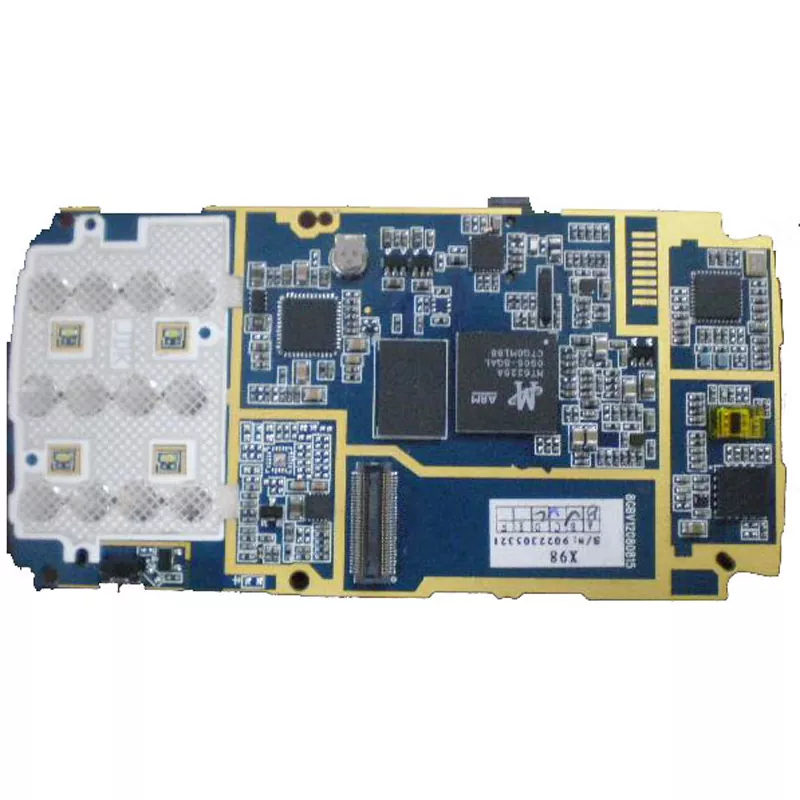
医療用PCBAボード
Hitech は、医療用 PCBA ボードを卸売できる中国の医療用 PCBA ボードのメーカーおよびサプライヤーです。プリント基板アセンブリ (PCBA) は、医療機器の製造において不可欠なコンポーネントとなっています。これらは、さまざまなプロセスや機能を制御する信頼性の高い効率的な手段を提供することにより、医療機器の機能において重要な役割を果たします。医療業界では、PCBA は監視および診断装置から手術器具や埋め込み型デバイスに至るまで、幅広い用途で使用されています。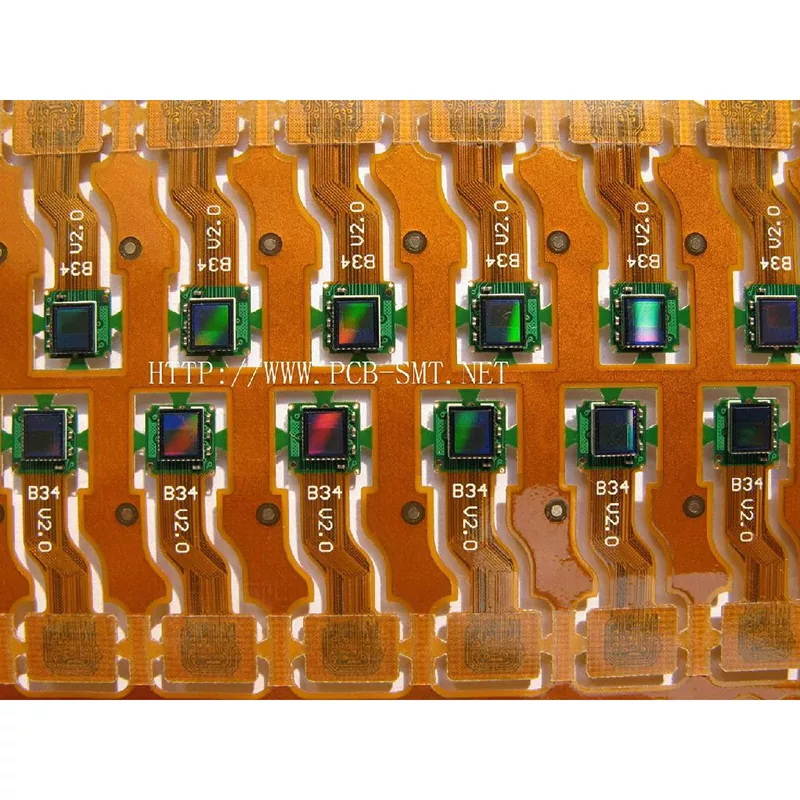
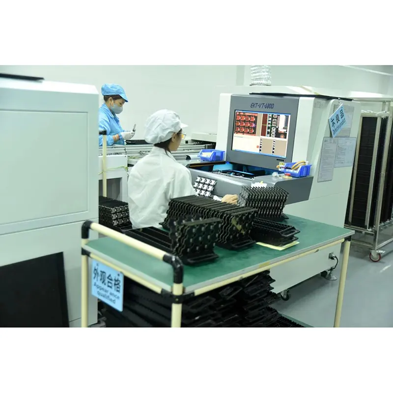
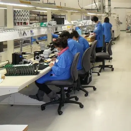
PCBA ボードのテストと品質管理
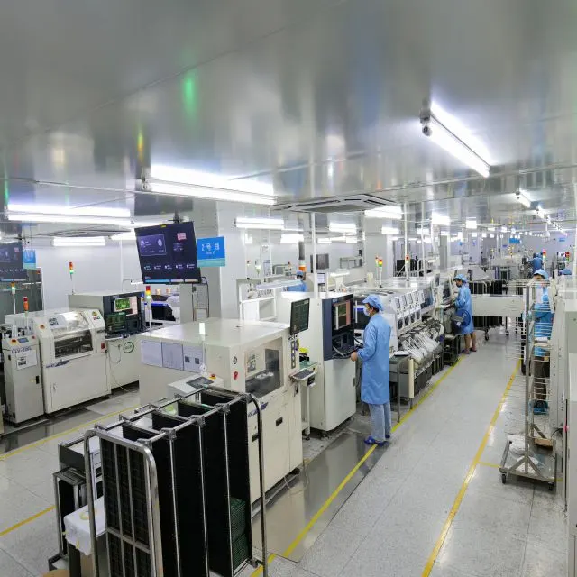
Hitech は、高品質の PCBA ボードのテストと品質管理を低価格で直接購入しています。プリント基板アセンブリ (PCBA) のテストと品質管理は、電子デバイスの製造における重要なプロセスです。これらのプロセスにより、最終製品が高品質で欠陥がなく、意図したとおりに機能することが保証されます。この記事では、PCBA テストと品質管理の重要性と、最終製品が必要な品質基準を満たしていることを確認するために使用されるさまざまな方法について説明します。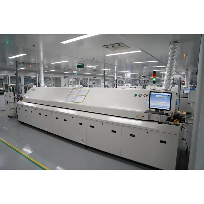
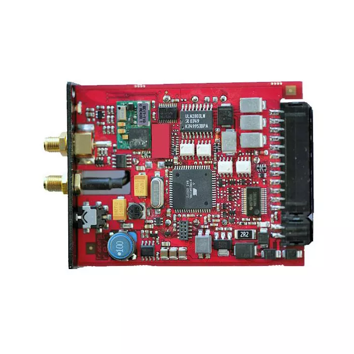
リフローはんだ付け PCB アセンブリ
Hitech は、高品質とリーズナブルな価格を備えた中国のリフローはんだ付け PCB アセンブリのプロフェッショナル リーダー メーカーです。はんだペーストを使用して表面実装部品を PCB に接合するために使用される方法です。リフローはんだ付けでは、PCB アセンブリを特定の温度に加熱し、はんだペーストを溶かして、コンポーネントと PCB の間に永久的な接合を作成します。このプロセスは非常に精度が高く、幅広い電子機器に使用される高品質で信頼性の高い PCBA の作成が可能になります。リフローはんだ付けは、PCBA の製造プロセスにおける重要な要素であり、最終製品が高品質で欠陥がなく、意図したとおりに機能することを保証します。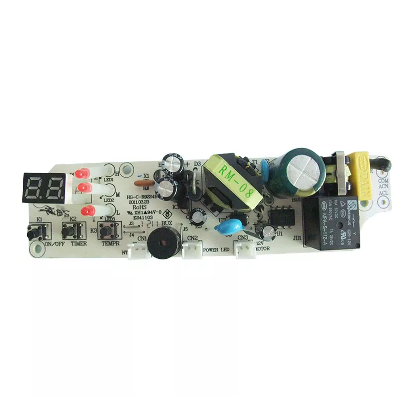
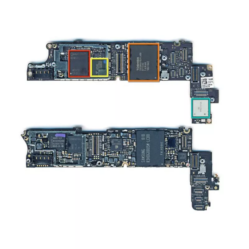
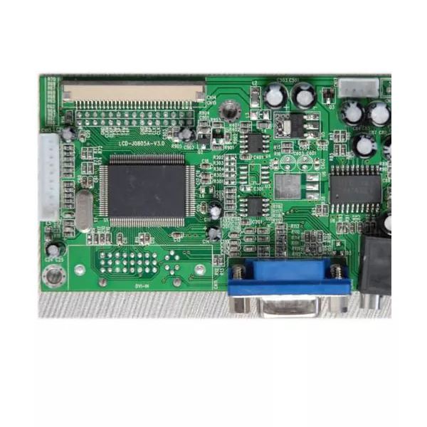
PCB レイアウト
プリント基板 (PCB) のレイアウトは、電子設計プロセスの不可欠な部分です。これには、最終製品が希望の仕様を確実に満たすように、コンポーネントを配置し、PCB 上にトレースを配線することが含まれます。 PCB レイアウトは電子設計プロセスにおける重要なステップであり、最終製品の性能、製造性、信頼性に影響を与える可能性があります。この記事では、PCB レイアウトの重要性と、それがプロジェクト全体の成功にどのような影響を与えるかについて説明します。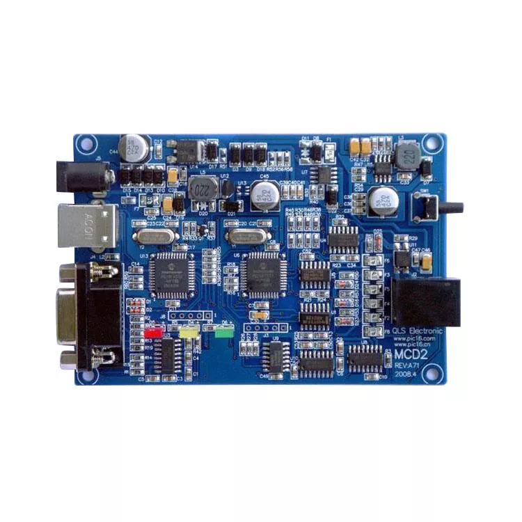
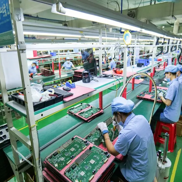
PCBA設計
今日のペースの速い技術環境では、電子デバイスの成功はプリント基板アセンブリ (PCBA) の設計にかかっています。完璧な PCBA 設計は、最適なパフォーマンスを保証するだけでなく、革新性、効率性、費用対効果を実現します。この記事では、PCBA 設計の世界を深く掘り下げ、その重要性、重要な考慮事項、製品開発にもたらす利点を探ります。あなたがエレクトロニクス愛好家であっても、経験豊富なプロフェッショナルであっても、この記事を読んで PCBA 設計の秘密を解き明かしてください。
LED PCBAボード設計
Hitech invites you to visit our factory to purchase the newest, best-selling, affordable, and high-quality LED PCBA Board Design. We are looking forward to working with you.
- 関連ブログ
- レビュー