- English
- Español
- Português
- русский
- Français
- 日本語
- Deutsch
- tiếng Việt
- Italiano
- Nederlands
- ภาษาไทย
- Polski
- 한국어
- Svenska
- magyar
- Malay
- বাংলা ভাষার
- Dansk
- Suomi
- हिन्दी
- Pilipino
- Türkçe
- Gaeilge
- العربية
- Indonesia
- Norsk
- تمل
- český
- ελληνικά
- український
- Javanese
- فارسی
- தமிழ்
- తెలుగు
- नेपाली
- Burmese
- български
- ລາວ
- Latine
- Қазақша
- Euskal
- Azərbaycan
- Slovenský jazyk
- Македонски
- Lietuvos
- Eesti Keel
- Română
- Slovenski
- मराठी
- Srpski језик

中国通信製品用PCBアセンブリおよびプログラミング用PCBAメーカー、サプライヤー、工場
Hitechは、中国の専門的な通信製品用PCBアセンブリおよびプログラミング用PCBAメーカーおよびサプライヤーです。当社の高品質通信製品用PCBアセンブリおよびプログラミング用PCBAは中国で作られているだけでなく、カスタマイズされた製品があります。私たちの工場へようこそ。製品を購入してください。
関連製品


人気の製品
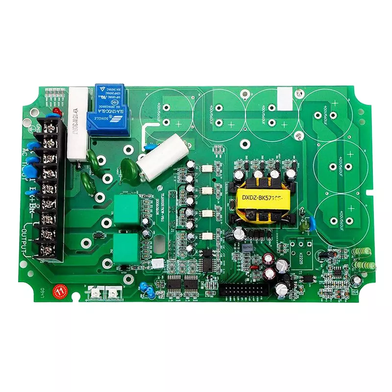
QFN PCB アセンブリ
高密度エレクトロニクスの未来エレクトロニクス業界は常に進化しており、新しい技術やイノベーションが日々生まれています。高密度エレクトロニクスにおける最新のトレンドの 1 つは、QFN (Quad Flat No-Lead) パッケージの使用です。これらのパッケージにより、PCB 上のコンポーネントの高密度化が可能になり、その結果、電子デバイスがより小型でより効率的になります。当社では、幅広い業界に対応する QFN PCB 組立サービスを専門としています。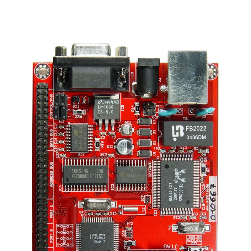
FR4基板
FR4 PCB (プリント基板) は、エレクトロニクス業界で最も広く使用されているタイプの PCB の 1 つです。これらは、ガラス強化エポキシ積層板の一種である FR4 と呼ばれる材料で作られています。 FR4 は、優れた電気絶縁特性、高強度、耐熱性と耐湿性で知られています。これらの特性により、FR4 PCB は家庭用電化製品、医療機器、産業機器などを含む幅広いアプリケーションにとって理想的な選択肢となります。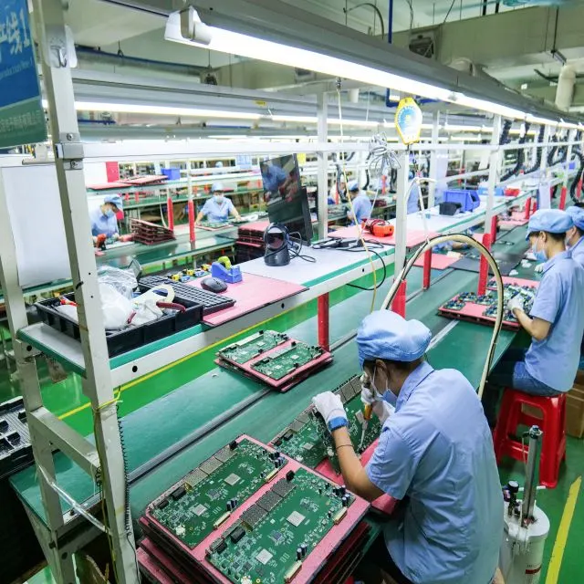
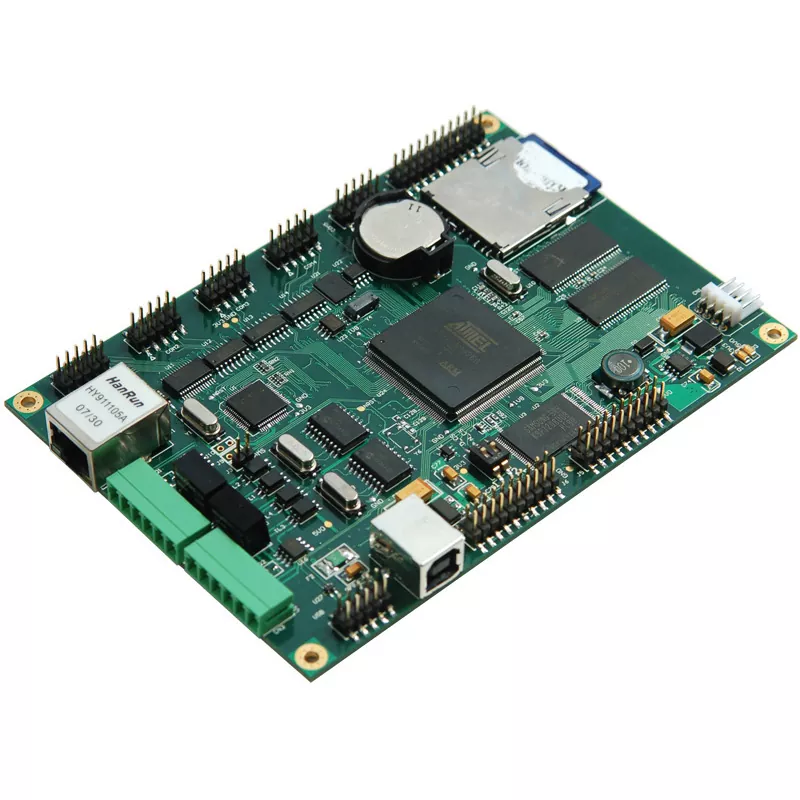
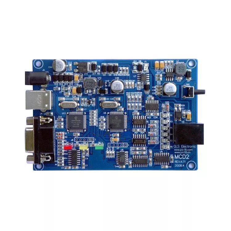
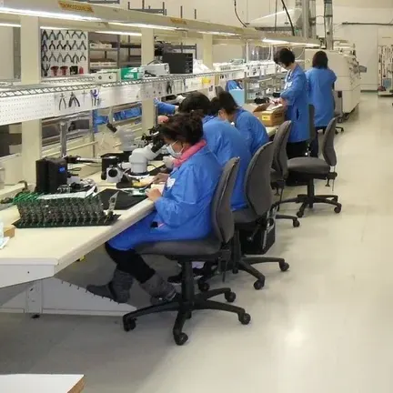
電子製造サービス
電子製造サービス(EMS)は、電子製品の製造をアウトソーシングするための完全なソリューションです。このサービスには、設計やプロトタイピングから最終アセンブリ、テスト、出荷まで、さまざまなアクティビティが含まれています。 EMSプロバイダーは、オリジナルの機器メーカー(OEM)および他の企業と協力して、電子機器の製造プロセス全体にワンストップショップを提供しています。
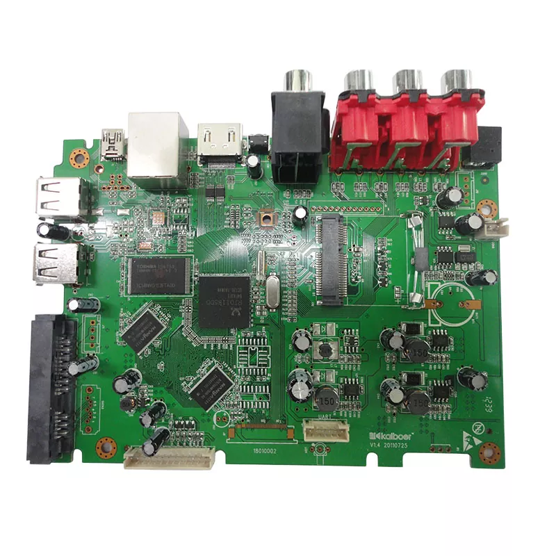
IoT PCBの設計と製造
Hitechで中国からIoT PCBの設計と製造の膨大な選択を見つけてください。協力を楽しみにして、プロのアフターセールスサービスと適切な価格を提供します。
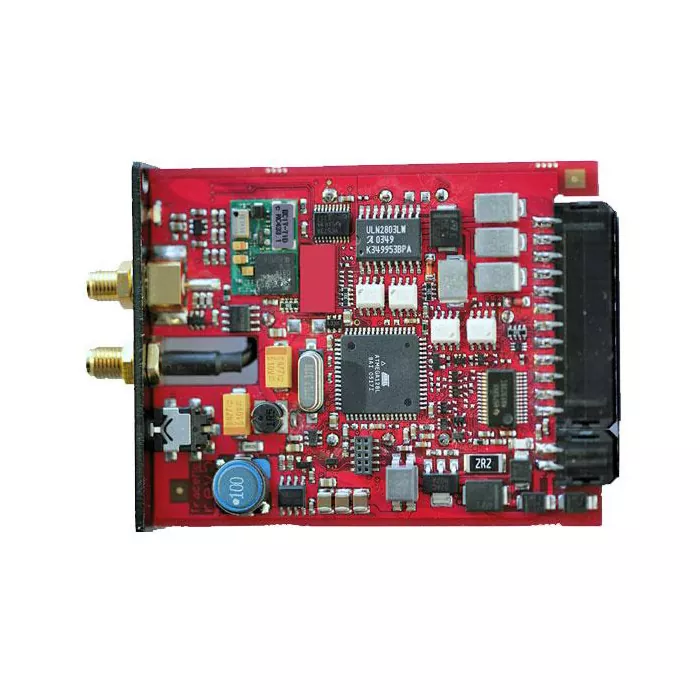
BluetoothトラッカーPCBAデザイン
One of Chinese manufacturer of Bluetooth Tracker PCBA Design, offering excellent quality at a competitive price, is Hitech. Feel free to get in touch.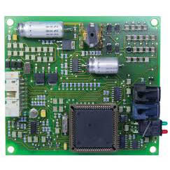
カスタム充電PCBA
今日のペースの速い世界では、電子デバイスに効率的で信頼性の高い電源が必要なため、高性能充電ソリューションが不可欠になります。カスタマイズ可能で高性能の充電に対する需要の高まりを満たすために、HITECH分野の革新により、PCBAのカスタム充電の開発が生まれました。これらの特殊な印刷回路基板アセンブリは、標準ソリューションのパフォーマンスを超えるパフォーマンスを提供するように設計されています。
- 関連ブログ
- レビュー